Product details
Product Overview
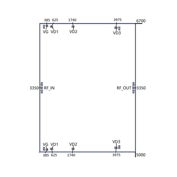
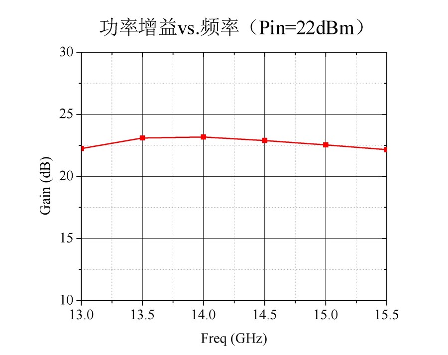
The RFSPA1207C-1216P30 is a GaN power amplifier chip covering 13–15.5 GHz, with 23 dB power gain, 45 dBm saturated output power and 32% PAE. It operates in both pulsed and CW modes. Chip size: 5.00 × 6.70 × 0.10 mm. All chips are 100% DC and RF tested on-wafer.
Key Features
13–15.5 GHz bandwidth
23 dB power gain with ±0.75 dB flatness; 32 dB linear gain
45 dBm saturated output power
32% power-added efficiency (PAE)
IMD3 −30 dBc @ Pout = 40 dBm (ICQ = 700 mA, two-tone spacing 5 MHz)
Operates in both pulsed and CW modes; 100% DC and RF tested on-wafer
Technical Specifications
| Model | RFSPA1207C-1216P30 |
|---|---|
| Product Category | MMIC Products |
| Device Type | GaN MMIC Power Amplifier Chip (bare die) |
| Frequency Range | 13–15.5 GHz |
| Linear Gain | 32 dB (typ) |
| Power Gain | 23 dB (typ) · flatness ±0.75 dB |
| Input / Output Return Loss | −7 dB / −7 dB |
| Saturated Output Power | 45 dBm (typ) |
| PAE | 32% (typ) |
| IMD3 | −30 dBc @ Pout = 40 dBm, ICQ = 700 mA, two-tone spacing 5 MHz |
| Operating Current | 3.5 A (typ) · +28 V @ 3.0 A (quiescent) |
| Chip Size | 5.00 × 6.70 × 0.10 mm |
| Thermal Resistance | 1.0 °C/W |
| Operating Modes | Pulsed and CW |
| Test Conditions | VD = 28 V (CW), VG = −1.6 V, Pin = 22 dBm, TA = +25 °C |
| Absolute Maximum Ratings | VDS +32 V · VGS −5 V · Pin +30 dBm · Tch +200 °C |
| RF / Bias Pads | RF_IN / RF_OUT: 100 × 120 μm² · VG: 100 × 120 μm² · VD1: 100 × 150 μm², VD2: 100 × 140 μm², VD3: 110 × 150 μm² · outline tolerance ±20 μm |
Assembly & Handling Notes
Store in a dry, clean N2 environment; the 6H-SiC substrate is brittle — handle carefully to avoid damage
Carrier CTE should be close to 6H-SiC (4.2×10⁻⁶/°C); CuMoCu, CuMo or CuW recommended; avoid voids between chip and carrier and ensure good heat dissipation
Eutectic bonding with AuSn solder (Au:Sn = 80%:20%), temperature ≤300 °C, time ≤30 s; avoid rapid temperature changes
Gold wires of 25–30 μm diameter recommended; bonding stage temperature ≤250 °C
Power sequencing: apply gate bias before drain bias on power-up; remove drain bias before gate bias on power-down
External capacitors C1 = 100 pF, C2 = 1000 pF close to the chip (within 500 μm); DC-blocking capacitors integrated at chip input and output
ESD precautions: wear a grounded anti-static wrist strap and ensure the sintering/bonding stages are well grounded