Product details
Product Overview
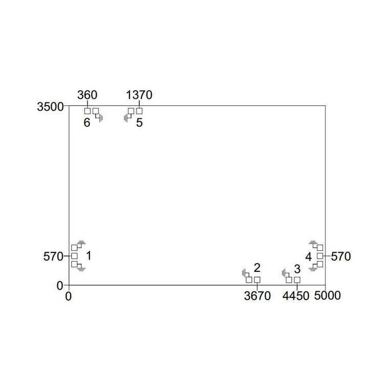
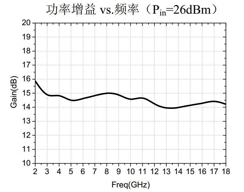
The RFSPA1261C-218P10 is a GaN power amplifier chip covering 2–18 GHz, with 14 dB power gain, 40 dBm saturated output power and 20% PAE. It operates in both pulsed and CW modes. Chip size: 5.00 × 3.50 × 0.10 mm. All chips are 100% DC and RF tested on-wafer.
Key Features
Wide 2–18 GHz bandwidth in a compact 5.00 × 3.50 × 0.10 mm die
14 dB power gain with ±1.0 dB gain flatness
40 dBm saturated output power
20% power-added efficiency (PAE)
Operates in both pulsed and CW modes
100% DC and RF tested on-wafer
Technical Specifications
| Model | RFSPA1261C-218P10 |
|---|---|
| Product Category | MMIC Products |
| Device Type | GaN MMIC Power Amplifier Chip (bare die) |
| Frequency Range | 2–18 GHz |
| Power Gain | 14 dB (typ) |
| Gain Flatness | ±1.0 dB |
| Saturated Output Power | 40 dBm (typ) |
| PAE | 20% (typ) |
| Input VSWR | 2.5 |
| Operating Voltage | +28 V @ 0.9 A (quiescent) |
| Chip Size | 5.00 × 3.50 × 0.10 mm |
| Operating Modes | Pulsed and CW |
| Test Conditions | VD = 28 V (CW), VG = −1.6 V, Pin = 26 dBm, TA = +25 °C |
| Absolute Maximum Ratings | VDS +30 V · VGS −5 V · Pin +30 dBm · Tch +200 °C |
| RF / Bias Pads | RF_IN / RF_OUT: 110 × 110 μm² · VG1, VG2, VD1, VD2: 110 × 110 μm² · outline tolerance ±20 μm |
Assembly & Handling Notes
Assemble and use in a clean environment; GaN material is brittle — handle with care and do not touch the chip surface
Use 2 bond wires (25 μm gold wire) for input and output, kept as short as possible (≤300 μm)
Sinter with 80/20 AuSn solder at ≤300 °C, as short as possible (≤30 s)
External capacitors C1 = 100 pF, C2 = 1000 pF (single-layer ceramic), with C1 placed as close to the chip as possible (within 500 μm)
ESD-sensitive device — take anti-static precautions during storage and use
Store in a dry nitrogen environment; do not clean the chip surface with dry or wet chemical methods